
Table of Contents
Introduction
Hey guys, welcome back to Techatronic. In this article, we are going to cover the 8085 microprocessor.
- The main function of a microprocessor is to perform several functions and decision-making for changes in the series of program implementations.
- The 8085 microprocessor is launched by Intel and is one kind of semiconductor device synchronized by the clock. This processor can be built with electronic logic circuits that are fabricated using the technologies like VLSI or LSI.
- This processor is an NMOS device and consists of thousands of transistors. It is an 8 bit general purpose processor that can deal with the memory of 64kb.
- It is also 100% software compatible with also on-chip clock generator in addition with external crystal oscillator.Now let’s see the pin diagram and the 8085 architecture.
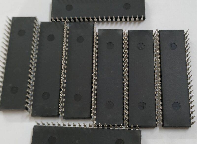
pin diagram of 8085 microprocessor
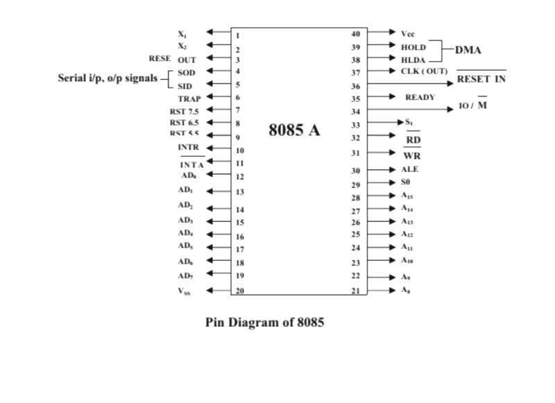
- PIN 1,2 : X1, X2 → These pins are connected to external crystal oscillator to make the internal clock generator work. The input frequency is divided by 2 to provide working frequency for the processor.
- PIN 3 : RESET OUT → This pins indicates that the CPU is being REST. This is an output pin, so it can be used as a working or indicating signal from the microcontroller to perform a task which should be done at the time when the microprocessor resets.
- PIN 4 : SOD → This is an output pin for the serial communication of the IC with the HOST to program the chip. It is similar to Tx pin of the many other microcontrollers.
- PIN 5 : SID → This i s an input also for the serial communication between the IC and the HOST to program the chip. It is similar to the Rx pin on various other microcontrollers.
- PIN 6 : TRAP → This is an INPUT pin which is sensitive to non-maskable RESTART interrupt also known as trap interrupt. It is recognized by the microprocessor at the same time as the INTR or RST interrupts. But this hast the highest order of priority among all interrupts.
- PIN 7-9 : RST(5.5, 6.5, 7.5) → These 3 pins are INPUTS pins for causing an immediate RESTART of the microprocessor at the instant. These can be masked and have high priority than INTR. For order of priority table view IC datasheet attached below.
- PIN 10 : INTR → This is the INPUT pin for creating a general purpose interrupt request. It is executed during next to the last clock cycle and during HOLD and HALT states. This can be controlled using software, as a result of which INTA will be issued. It has the least priority in the interrupt table among all other interrupts.
- PIN 11 : INTA → This is the OUTPUT pin which is activated as a result of when an INTR is accepted. This can be used as the signal of other task of the other microcontrollers or IC’s which need to be performed at that time. so, by this 8085 pin diagram you will definately find the information.
- PIN 12-19 : AD0-AD7 → These are the MULTIPLEXED ADDRESS/ DATA BUS, i.e., used to perform INPUT/OUTPUT functions.
- PIN 20 : VSS → Ground pin connected to lower potential of the power supply.
- PIN 21-28 : A8-A15 → These are OUTPUT pins which are ADDRESS BUS which holds the 8bit address of the memory.
- PIN 29, 33 & 34 : S0, S1 & IO/M → These are OUTPUT pins which are used to tell the status of the MACHINE CYCLE. These 3 pins in ever truth table format represents the current status of the IC, you can either use LEDs or something else to check for status. For more info, view its datasheet for more info.
- PIN 30 : ALE → ADDRESS LATCH ENABLE is the OUTPUT pin which occurs during the first clock state and enables the address to get latched(store) into the on-chip latch(storage) of peripherals.
- PIN 31 : WR → This WROTE CONTROL, OUTPUT pin(low signal) indicates that the data is to be written on to the databus or the selected memory location.
- PIN 32 : RD → This READ CONTROL, OUTPUT pin(low signal) indicates that the Data Bus is ready for data transfer i.e., to read the selected memory location or I/O device
there is one more microprocessor same as this 8086 microprocessor
- PIN 35 : READY → This is the INPUT pin which is HIGH during the Read and Write cycle, that indicates that the bus and memory is ready to send or receive data. If this pin is low that the CPU will wait for the pin to go HIGH until the Read and Write Cycle completes.
- PIN 36 : RESET IN → This is the INPUT pin which sets the program counter to 0 and resets the interrupt Enable and HLDA Flip-Flops. It should be kept high for at least 3 clock cycles. Also, the CPU will be in reset state during the time the reset in signal is applied. 8085 architecture is easy to learn by this pin diagram.
- PIN 37 : CLK → This CLOCK pin is OUTPUT for the System Clock. Its time period is twice as that of the crystal oscillator input time period.
- PIN 38 : HLDA → This HOLD ACKNOWLEDGE, OUTPUT pin indicates that the CPU has received an HOLD request which indicates that it will clear the bus in the next clock cycle.
- PIN 39 : HOLD → Thin INPUT pin is used to send a signal to CPU which helps CPU determine that another master devices is requesting the address and data busses. Upon receiving this request, CPU clear the both busses ASAP after completion of current data transfer.
- PIN 40 : VCC → This is the power supply pin which should be given +5V in order for the IC to work.
- So we are done with the pin diagram of the 8085 microprocessor. You can also read about 555 timer IC and 741 operational amplifier IC.
Interrupts in 8085 Microprocessor
The 8085 microprocessor has a total of 5 interrupts. TRAP, RST 7.5, RST 6.5, RST 5.5, and INTR are interrupted present in 8085. TRAP is on pin number 6, RST 7.5 is on pin number 7, RST 6.5 is on pin number 8, RST 5.5 is on pin number 9, INTR is on pin number 10.
Block diagram of 8085 microprocessor
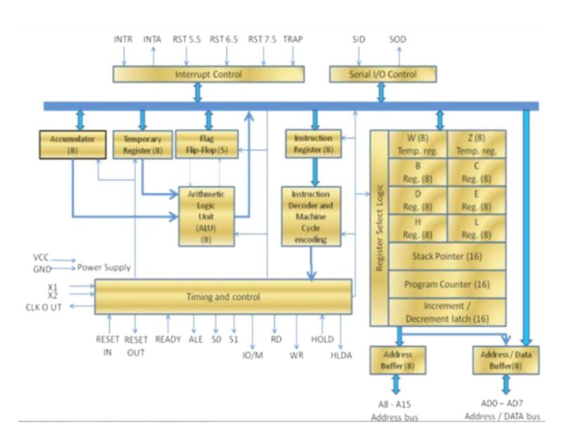
Now let us discuss the flag registers present in the 8085 microprocessor. Sign flag, zero flag, carry flag, auxiliary carry flag, and parity flag. These flags are set and reset continuously by the microprocessor itself during the execution of given commands. It has some special purpose registers also. We are going to study them in detail.
- Accumulator: Use to store 8 bit data and it is a part of ALU.
- General purpose registers: There are 6 general purpose registers (B, C, D, E, H, and L). They are of 8 bits.
- Stack pointer: Its function is similar to a stack which is constantly increse and decrease.
- Instruction register: It holds the operation code of the current instruction of a program during an operation.
- Program counter: It holds the address of the next instruction.
- Temperory register and PSW (program status word) register.
Advantages:
- Unlike 8086 it can easily be programmed using software.
- It has slightly low cost than, 8086 microprocessors
- It has16-bit address bus, which can address upto 64 KB
- 3MHz,5MHz & 6MHz frequency can be selection depending upon the requirement.
Disadvantages
- Low memory available for storage.
- Less number of I/O operation can be performed as compared to 8086.
- It has 3 MHz of default frequency, which is quite slow for fast computation performing task.
FAQ
Q. What is the working voltage level of the 8085 microprocessor?
It has a working voltage level of 5V. Above or below, this may result in damage or malfunction of the IC.
Q. In which language the 8085 Microprocessor is programmed?
It is programmed in assembly language, the sample programs and instruction set can be found online as open source.
Conclusion
We hope that you understand all the facts that we discussed above regarding the 8085 microprocessor. If you have any doubts related to this post then you can ask them in the comments section given below. You can also check out projects on Arduino and Raspberry pi.
Happy learning!