Table of Contents
Introduction
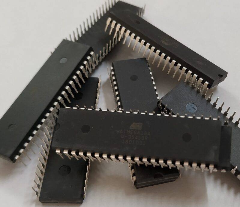
Hey guys, welcome back to Techatronic. Today, we will discuss some facts about the intel 8086 microprocessors.
- The 8086 microprocessor is a 16-bit microprocessor designed by intel. It has a 20 bit address bus and 16 data lines and can provide storage upto.
- This microprocessor can perform many operations, and we can program it for performing specific functions. It has an instruction queue, which is capable of storing 6 instructions bytes from the memory, resulting in faster processing.
- 8086 microprocessors can come in many variants, such as 8086-1 and 8086-2. The clock speed of 8086 is 5 MHz, 8086-2 is 8MHz and 8086-1 is 10 MHz. It consists of 29,000 transistors.
- It was mainly designed for assembly languages and high level programming languages. Also, it can be operated in both single processor and multiprocessor configurations for performing task more accurately and speedily.
- It was the first 16-bit processor having 16 bit ALU and 16-bit external data bus. Now let us see the pin diagram for the 8086 microprocessor. You can also check articles on Arduino and basic electronics.
8086 microprocessor pin diagram Explanation
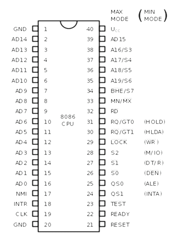
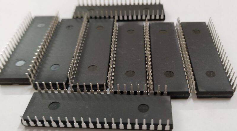
- 8086 microprocessors works on voltage level 5 V DC power supply. It comes in a 40-Lead Cerdip and Plastic Package, with 20 on each side. So, here we are going to explain you the 8086 pin diagram in very easy way. now you can easily learn.
- PIN 1 & 20 are GND Pins which should be connected to low potential of the power supply or to the ground of the whole system.
- PIN 2-16 & 39 : AD15-AD0, These are ADDRESS DATA BUS. These lines are used for I/O function with time multiplexed memory. These are active high and 3-state during interrupt acknowledge.
- PIN 17 : NMI, NON-MASKABLE INTERRUPT. This pin is for creating a type 2 interrupts, which occurs due to a triggered input. This cannot be done internally with software as you have to make it happen physically from LOW to HIGH, but the interrupt is internally synchronized.
- PIN 18 : INTR, INTERRUPT REQUEST. This is a level triggered input (active HIGH) which usually occurs at the last clock cycle of each instruction to check whether or not the processor into interrupt acknowledge operation mode. This can be set internally with the help of software by resetting the interrupt enable bit, also the interrupt is synchronized internally.
- PIN 19 : CLK, CLOCK. This pin provides the clock signal for the processor and bus control. It is asymmetric with 33% duty cycle to provide optimized internal timing.
If you want to learn the working and 8086 architecture you need to see the working of each pin. which can also help you to learn the coding for this processor.
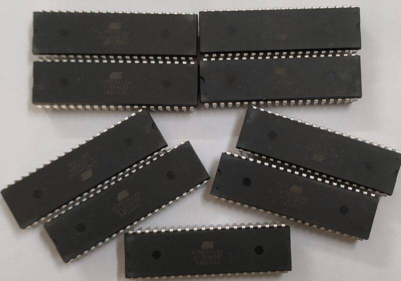
- PIN 21 : RESET. This pin is used to reset the processor from whatever state it is in. The signal should be active high for at least 4 clock cycles. When the pin is pulled low, it restarts execution from the beginning as in the code or program, all this is internally synchronized.
- PIN 22 : READY. This pin reads the ready signal that indicated that the addressed memory or I/O has completed the data transfer. the signal is synchronized by the 8284A Clock Generator along with the address bus to from READY. The signal is active HIGH, but it is not synchronized also it may malfunction if signal timings are not correctly matched.
- PIN 23 : TEST. This input is detected by a “WAIT” instruction in 8086 microprocessor. If the input is LOW execution of the program continues, else the processor will wait or delay the task until the signal is LOW. The input is synchronized internally during each clock cycle at the leading edge (start or LOW to HIGH) of CLK signal.
- PIN 24, 25 : QS1, QS0; QUEUE STATUS. These two pins are used to determine the queue status. This signal is valid during the CLK cycle after which the queue operation is performed. These are usually used for external visualization of tasks performed by the processor. These pin functions only in maximum mode.
- PIN 26-28 : S2—S0. These pins give output which floats to 3-state OFF in hold acknowledge. These have a truth table for all type of combinations, which you van refer to datasheet attached below on pg4. These pin also functions only in maximum mode.
- PIN 29 : LOCK. This pin output indicated the supremacy of bus control over other system bus masters. The signal is active low and remains low until completion of the next instruction.
- PIN 30,31 : RQ/GT, REQUEST/GRANT. These pins are bidirectional and used by other bus master to request the control over bus at the end of the current bus cycle also they have internal pull-up resistor.
- PIN 32 : RD, READ. This output pin indicated that the processor is performing a memory size of 8086 microprocessor or I/O cycle, which totally depends on the state of S2 pin. This pin is used to read devices, which resides on the 8086 local bus.
- PIN 33 : MN/MX, MINIMUM/MAXIMUM. This is used to set the processor in either MINIMUM or MAXIMUM mode. And pins function accordingly.
- PIN 34 : BHE/S7, BUS HIGH ENABLE/STATUS. This pin provides a signal to enable the data on the most significant half of the data bus (D15-D8).
- PIN 35-38 : A19/S6-A16/S3, ADDRESS/STATUS. These pins are the most significant line for memory operations during t1. During I/O operation, these pins are LOW.
- PIN 40 : VCC. This is the power pin which should be connected to high potential of the system. The working voltage level of the IC s 5V, and it should not exceed that.
- You can also check about what 555 timer IC and 741 Op-Amp IC are and how they work.
Register Set of 8086 Microprocessor
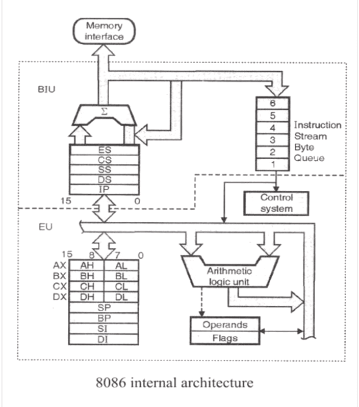
- There are some flag registers such as carry flag, auxiliary carry flag, parity flag, zero flag, sign flag, and overflow flag registers.
- These registers can be set and reset automatically during the execution of the program to hold the values of the final outcomes.
- These are also known as conditional flag registers.
- Apart from that intel 8086 microprocessor also have some control flags such as trap flag, interrupt flag, and direction flag register.
- Now let us discuss some general purpose registers.
- AX (accumulator) is used to store operands.
- BX (base register) is used to store starting base address.
- CX (counter) is used in loop instructions.
- DX is used to hold the I/O port address.
- Register pairs: AH and AL, BH and BL, CH and CL, DH and DL.
Advantages & Disadvantages:
Advantages:
- Different versions available for requirements, which affects the speed of the overall working of code.
- Working voltage level is from 2V-5V, which offers a wide variety of other microcontrollers which can be used with it.
- 16-bit processor which helps in tasks which require fast require and ideal for them
- Multibus compatible interface
Disadvantages:
- The size or the package of the IC is not very common, so the IC base, or it can’t be soldered on normal perfboard easily sometimes.
- This microprocessor is a bit costly and can be replaced with nowadays most common board that is Arduino and others.
- Te programming of these needs some special software that can program this in assembly language over the most common nowadays like Arduino IDE or python.
FAQ
Q. What is MIN/MAX mode in 8086 microprocessors?
MIN/MAX is the mode which you can switch between requires for the task also in both modes certain pins work differently as mentioned above. Some pins functions are not mentioned as they are in the datasheet attached above.
Q. Which language is used to communicate with 8086 microprocessors?
Assembly language is used to communicate between 8086 microprocessors, like with other bus microcontrollers or microprocessors.
Q. Voltage range of the 80886 microprocessor.
It works between 2V-5V, voltages above or below can either damage the IC or result in a malfunction of it. so it is highly recommended to use the voltage within is within this range.
Conclusion
We hope that you understand entirely the pin diagram and operations of an 8086 microprocessor. If you have any doubts regarding this post, do let us know in the comments section below. Also, do check out more articles on Arduino and Raspberry Pi.
Happy Learning!

