

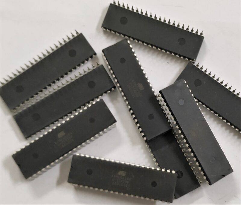
Hey guys, welcome back to Techatronic. In this article, we will learn about the 8051 microcontroller and memory organization in it. 8051 is an 8-bit microcontroller designed by intel in 1981. It has a bidirectional data bus of 8 bits and a 16-bit unidirectional address bus.
There are two 16 bits timers/counters and four 8 bits input and output ports. The internal data memory of 8051 is divided into two groups. There are a set of 8 registers and a scratchpad memory. some people called it or search it by 8051 microprocessor. it is a microcontroller, not a microprocessor.
These eight registers are R0 to R7. It has 4 Kb of ROM and 128 bytes of RAM. You can read our articles on IoT and basic electronics. So let us start
Table of Contents
8051 Pin Diagram
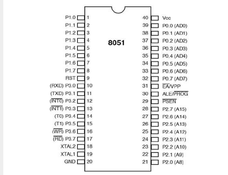
8051 Pin Description
It is the very famous 8051 microcontroller along with Arduino and ESP Family. But unlike both family It comes in DIP package and is a single or main component which requires to be programmed.
This 8051 can easily be programmed either using Arduino ICSP or using any other FTDI custom software. Tutorial for programming is also available, you can view it from Programming in 8051.
It has 4 ports, 2 timers and 1 serial which can be used, But as it is very old controller no Modern communication like SPI, I2C or any other can be used.
Further we’ll discuss some pins and their functions, For more detailed information you can always refer to its datasheet.
PIN 1-8 : These are 8051 port pins, (PORT 1) with 8-bit Bi-Direction I/O, pull-up resistors and Schmitt trigger.
PIN 9: It is the rest pin which is used to reset the microcontroller. To reset the chip, you have to make this pin HIGH for two machine cycles. Also connect an external capacitor with Vcc to this pin for power-on reset.
PIN 10-17:These are also port pins (PORT 3) like 1-8 with 8-bit Bi-Direction I/O, pull-up resistors and Schmitt trigger. But unlike them these pins are for some special function which are discussed further:
PIN 10 (RXD), : This is the serial Input Pin for receiving data during programming the chip.
PIN 11 (TXD), : This is the serial Input Pin for transmitting data during programming the chip.
PIN 12 (INT0), : External interrupt
PIN 13 (INT1), : External interrupt
PIN 14 (T0), : Timer 0 external input
PIN 15 (T1), : Timer 1 external input
PIN 16 (WR), : External data memory write strobe
PIN 17 (RD), : External data memory read strobe
PIN 18-19: these are the XTAL pins which are connected to external crystal oscillator.
PIN 20: GND Pin connected to ground of the power supply.
PIN 21-28: These are also port pins (PORT 2) like other two with 8-bit Bi-Direction I/O, pull-up resistors and Schmitt trigger.
PIN 29 (PSEN): Program Store Enable, This pin is activated during reading memory strobe from external memory.
PIN 30 (ALE/PROG): Address Latch Enable/Program Pulse, output pulse for latching the low byte of the address during access to external memory. In normal operation, ALE is emitted at a constant rate of 1/6 the oscillator frequency, and can be used for external timing or clocking.
PIN 31 (EA/VPP): External Access Enable/Programming Supply Voltage, This pin is pulled low to enable the device to fetch code from external program memory locations.
PIN 32-39: These are PORT 0 pins which are open-drain, bidirectional I/O port with Schmitt trigger inputs.
PIN 40: This is the Vcc pin connected to high potential of the power supply.
it is a microcontroller, not a microprocessor. to understand the difference between the microprocessor and microcontroller. you need to read our embedded system article.
Register Set of 8051 Microcontroller
- Accumulator: This acts as an operand register, the accumulator register is a general purpose register to hold the results of the arithmetic and logic operations.
- B register: Used to store one of the operands for multiply and divide instructions. It is also a general purpose register.
- Program status word (PSW): This set of flags contains the status information and is considered as one of the special purpose register.
- Stack pointer: Incremented before the data is stored onto the stack using push or call instructions. This register contains 8 bit stack top address.
- Data pointer (DPTR): It contains a higher byte DPH and a lower byte DPL of a 16 bit external data RAM address.
- Serial data buffer: It contains two independent registers, one is a transmit buffer which is necessarily a parallel in serial out register, the other is called a recieve buffer which is a serial in parallel out register in 8051.
- Timer registers: These two 16 bits registers in 8051 can be accessed as their lower and upper bytes.
- Control registers: These are special function registers IP, IE, TMOD, TCON, SCON contain control and status information for interrupts and special ports.
- Program counter: It is a 16 bits register which points to the address of the next instruction to be executed.
Memory Organization in 8051
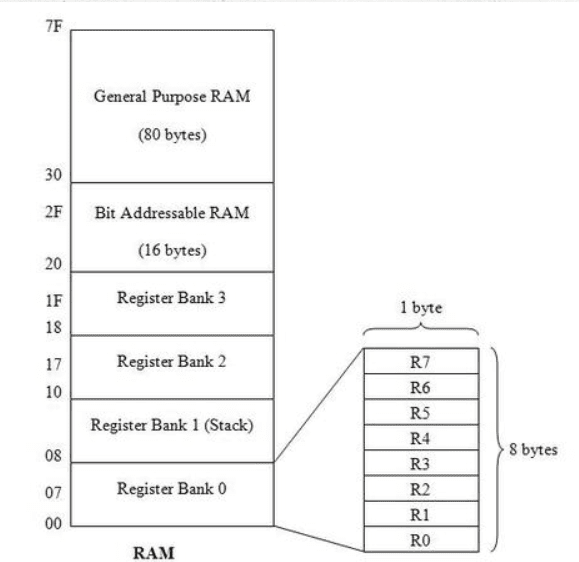
The memory organization in 8051 microcontroller is separated into program memory (ROM) and data memory (RAM). The program memory is used for storing the program to be executed i.e instructions. The data memory is used for storing temporary variable data and intermediate results. The internal RAM of 8051 is organized in three areas.
- Working registers: These are organized as 4 banks of 8 registers each and each register can be addressed by name or its RAM address. Bits RS0 and RS1 in the PSW will determine which bank of the register is currently in use. There are four banks starting from address 00H to 1FH.
- Bit addressable registers: These are used only when the program need to remember any binary event. and each bit has its own address. Starting from 20H to 2FH.
- General purpose RAM: Area above bit area, from 30H to 7FH, addressable as bytes.
Conclusion
We hope that you understand the working of an 8051 microcontroller and its memory organization completely. If you have any doubts regarding this post then use the comments section which is given below. Also, do check out more articles on Arduino and Raspberry Pi.
Thanks for learning