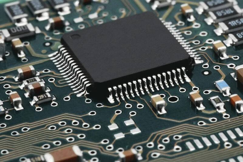
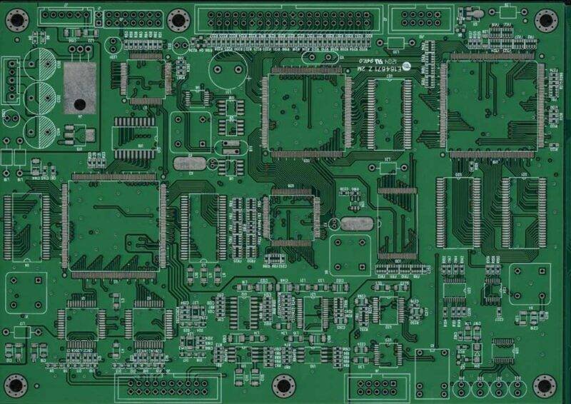
Printed Circuit Boards or PCBs are ever-present in the electronic world. Whether you are using a simple electronic gadget or a complex one, you will probably find a PCB in one of them. However, many people do not understand the technology behind PCB manufacturing.
Here are the basics of PCBs, from design to component and assembly, to have a good idea of how PCBs are made.

Table of Contents
The basics of a PCB
PCB is a laminated board that consists of thin strips of a conducting element like copper. Printed Circuit Boards have two functions. The first is to affix electronic elements in designated areas on the board. The other function of a PCB is to offer reliable electrical connections between the element’s terminals.
Various types of PCBs are found in several electronic gadgets. There are single-sided PCBs, double-sided PCBs, multilayer PCBs, Rigid PCBs, Flex PCBs, and Rigid-flex PCBs, among many others.
Multilayer printed circuit boards are the most popular because they allow a much higher component density. More than two copper planes can be used in complex applications.
The copper attached to the board is known as traces. They allow the electrical charge to pass through the board. This provides power to various elements that are situated on the PCB. These copper traces work as wires to guide the electricity to the right destination.

The Layers of a PCB
As explained above, there are various types of PCBs. However, the simplest type of printed circuit board is the single-sided PCB or single-layer PCB. The boards have one copper layer.
A solder mask and silkscreen are at the top of the copper layer. The green color that makes most printed circuit boards recognizable is the solder mask. Its work is to insulate the copper from any metal parts that can by accident come into contact with it.
Nevertheless, some parts of the metal that need to be soldered might remain exposed. Here is where the silkscreen comes in. The silkscreen sits on the solder mask and has numbers and letters. The numbers and letters were drawn, making the board assembly easier.
When copper traces are installed on both sides of the board, the printed circuit board is a double-sided PCB or double-layer PCB. A double-layer PCB is a bit more complex than a single-layer PCB.
Then a board becomes more complex when extra layers are added to the original design. The new layers have their copper trace formations making the design complex but can be used on bigger devices.
The board is a bit complex because the copper connections cannot cross one another without a path of electrical charge being compromised. Hence, a multilayer PCB is created.
A multilayer PCB is created for advanced electronics. By incorporating multiple layers, the boards increase functionality. In addition, it leads to the manufacturing of reliable products. Moreover, multilayer PCBs can be made in both rigid and flexible constructions.
Manufacturing printed circuit boards, especially multilayer PCBs, involves a lot of processes, such as CNC milling, hot pressing. For instance, alternating layers of prepreg and core materials are combined into a single unit.
The components
Printed circuit boards are complex things made up of various elements. Without the major components, the PCB cannot function as expected. Hence, PCB components are the essential organs of the board.
Even a component of the board has a different function. In addition, their unique qualities make the board fit for its intended purpose. However, it all depends on the electronic item or the device the PCB is designed for.
During the manufacturing of the PCB, these components are needed to perform their functions and ensure that the board is reliable. They consist of a range of electronic parts that include:
*Battery – this one provides the voltage to the circuit.
*Resistors – they control the electric current as it goes through them. The resistors are color-coded to define their value.
*LED – the Light Emitting Diode is a component that lights up when a current flows through it. It only allows the current to flow in one direction.
*Transistor – another important component of the PCB is the transistor. Its work is to amplify the charge.
*Capacitators – these are other vital components of PCB. They harbor electrical charge.
*Inductor – an inductor stores charge, stops, and changes in current.
*Diode – diode is a crucial element that allows current to go in one direction only. Hence, it blocks the other.
*Switches – it acts as a switch to either allow the current or block based on whether it is open or closed.
PCB Assembly
The above components are attached to the board to make it a printed circuit board. However, there are various ways to attach the elements. For instance, an engineer can choose to use the through-hole or surface mount to attach the elements.
The assembly is vital in PCB manufacturing because the engineers need to follow a schematic pattern. Through the schematic pattern and using the numbers on numbers found on the silkscreen, they use solder to attach the components.
However, since it is a complex process, the engineer must be very careful when soldering. Moreover, solder is a metal that can melt, making it easy to manipulate. The elements are well attached because any stray blob that is out of place or touches other metal elements can make the circuit to short.
This can be very dangerous and cause a small explosion or fire. Therefore, all the components need to be installed correctly. When well installed, the PCB will be ready to be used.
PCBs are used in various areas, including healthcare equipment, technology devices, military use, and consumer products, including television, phones, and others.
Summary
Now you know a printed circuit board’s basic design, components, and constructions. However, this is just a simple overview since PCB manufacturing is complex. From design to manufacturing, there are many stages involved for you to have a complete printed circuit board.
